User Guides
Our User Guides provide step-by-step instructions on how to use our free online smart tools and other available software.
If we lose boards during manufacture, we immediately launch a top-up order. We push this through production to try to meet the original delivery date. The new order has the extension –E1, so you can see if there’s been a reload on your order by checking the Running orders menu. If we lose boards at final inspection, then we immediately reload. Depending on the type of PCB, a remake is typically completed in 2 working days.
Sample check.
For each sample check, the number of samples to be tested is laid down by our QA department. This number is based on the size of the order and more than 30 years of manufacturing experience.
We use Eurocircuits’ standard tolerances unless the customer has requested special tolerances. For standard tolerances, please see our page “Tolerances on PCBs“.
For more information, you can also see our page “Understanding Manufacturing Tolerances on a PCB“.
Sample check.
The standard tolerance based on the laminate manufacturers’ specifications is +/- 10%. If there is a gold edge-connector, the measurement is always taken there.

Sample check.
We measure the finished hole size using a measuring microscope or a tapered probe with a read-out dial. The hole size tolerances depend on the type and size of the hole.

For more information, please see our page “Tolerances on PCBs“.
We check where needed.
If any boards are not flat, then we measure the bow and twist. For more information and some hints on designing to avoid bow and twist, go to our dedicated blog “Bow and Twist in Printed Circuits” and “eC-Glossary“
Sample tape test.
We use tape tests to test the adhesion of legend ink, soldermask, surface finish and copper. We press a strip of pressure-sensitive tape across the test area and then pull it off sharply. There should be no bits of legend ink, soldermask, surface coating or copper adhering to the tape.
100% visual inspection.
The PCB must be clean and free from any damage, scratches, fingerprints, dust etc. All design features must be present (holes, pads, tracks, slots and cut-outs, profiling for panels etc.)

100% visual inspection.
The base material must be correct to specification and show no defects (delamination, measling (white spots), inclusions etc.).
For more information, please visit our page “What is FR-4 or FR4“.
100% visual inspection.
All copper tracks, pads, planes must be present and of correct size to IPC specifications, and not over- or under-etched. To ensure that track widths are correct we use etch-compensation, that is, we increase the track widths on the phototools used to print the boards by the amount that the track will be reduced when it is etched (For more information, please see our page “Data Preparation“). Any nicks (“mousebites”), pinholes or scratches must also be within IPC specifications (For more information, please see our page “What is track width“.)
The isolation distance “track to track” (TT), “track to pad” (TP), and “pad to pad” (PP) must be correct to IPC specifications. There must be no shorts between copper features or open circuits (these will have been detected by electrical test). The inner layers must be correctly aligned to the outer layers. This has been checked at electrical test. There must be no inner layer copper exposed at the board edge (we normally cut back copper planes to ensure adequate clearance).
Sample check.
100% visual inspection.
The copper surface under the soldermask must be free of any damage, pitting, oxidisation, staining or burning.

Sample check.
We measure copper thickness using specialist measuring instruments. We have separate probes to measure the copper thickness on the surface of the PCB and through the holes. The copper on the hole walls must be minimum 20 microns thick. The main inspection is immediately after plating (see Part 1). At final inspection we measure a further sample.
100% visual inspection
Plated-through holes must be drilled right through and clear of any obstruction (glass fibres from the laminate, trapped dirt etc.). There must be no defects in the plating through the holes (voids, cracks, plating detached from the wall of the hole etc.). A complete break in the plating will have been detected at the electrical test stage and the board scrapped.
For more information, please see our page “What is the Micro Section of a PTH“.
100% visual inspection.
They must be clean and clear of any obstructions or contamination (glass fibres, plating etc.).
100% visual inspection.
Holes specified for via-filling must be completely closed, though the soldermask need not completely fill the hole.
Sample test.
Poor soldermask adhesion or curing is detected by the sample tape test described under Para 10.
Sample test.
Poor legend adhesion or curing is detected by the sample tape test described under para 10.
100% visual inspection.
The colour must be correct and the text legible without smearing. The marking should be cut back from the edge of the soldermask window by 0.1 mm. The legend must be correctly registered.
For more information, please see our page “What is the Legend of a PCB“.
100% visual inspection.
The soldermask must be of the correct colour and free of dirt or damage (some minor repairs are allowed). There must be no soldermask or soldermask residue contaminating pads to be soldered. It must be correctly registered.
For more information, please see our page “Soldermask“.
100% visual inspection.
The peelable soldermask must be a continuous layer 0.25 mm thick, free from dirt or damage and with no visible separation from the board surface. There must be no residual contamination elsewhere on the PCB.
100% visual inspection.
Eurocircuits’ order number, UL marking and any other special marking requested by the customer must be in the designated location and on the designated layer (typically the legend layer) as specified in the customer’s order.
Sample check on all finishes.
Poor surface finish adhesion is detected by the sample tape test described under Para 10.
100% visual inspection.
The surface must be flat and even across the PCB without any non-wetting. Component holes must not be narrowed or blocked. A few via holes may be blocked if they are not covered by soldermask.
Sample checks.
100% visual inspection.
The finish must cover all exposed copper and have the same colour across the PCB. There must be no discolouration even in the holes.

Sample check.
100% visual inspection.
Must not be tarnished or blackened. Finished boards are wrapped in “silver save” paper to avoid any oxidisation of the silver.
Sample test.
A sample is taken from every multilayer job and immersed in molten solder for a defined length of time. It is then checked for any delamination, blistering, solder-mask lifting etc.
Sample test.
A sample is immersed in molten solder for a short time. The surface must be completely coated with solder with no de-wetting or non-wetting.
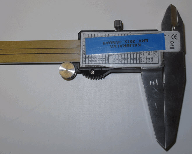
All measuring equipment is regularly calibrated back to national standards.