User Guides
Our User Guides provide step-by-step instructions on how to use our free online smart tools and other available software.
Written by Saar Drimer. 08/11/2024
Our new HDI pool allows customers to use microvias between layers L1-L2 and L2-L3 (or, alternatively, L6-L7 and L7-L8). Since the PCB is manufactured with our standard technology parameters, has two microvia runs, and the HDI (High Density Interconnect) is only applied to a part of the board, our solution, sometimes called ‘partial’ or ‘hybrid’ HDI, is cheaper than ‘full’ HDI. So when we want to use a single fine-pitch BGA – that perhaps comes in no other package – it doesn’t necessarily mean a very expensive board. In this article we’ll cover some techniques our customers may use to maximise the use of what the HDI pool can offer.
It’s hard to confidently know if a design with a BGA will be routable, and with how many layers, before trying. There are a lot of factors that make it possible or impossible: the PCB technology and assembly restrictions; the number of routing layers available; the amount of pins in the package (not all BGA arrays are ‘full’); how the pins are arranged (a cluster of power pins is helpful); how many pins are used by the design (many designs won’t have all pins of a microcontroller used, for example); and, the placement of the rest of the components relative to the pin-out of the BGA (if a memory interface bus is all over the array, for example, routing gets harder).
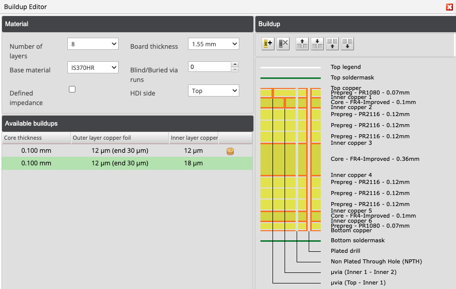
For the PCB technology and assembly restrictions we have the two HDI microvia runs mentioned earlier, and our Pattern classes which determine widths, clearances, pad and hole sizes, etc.; these are shown in Figure 1. We only support staggered microvias, where the holes are non-overlapping and have a minimum clearance of 0.010 mm (10 µm). (Conversely, this means that we do not support stacked vias). For the amount of layers, it’s simple: the HDI pool has only one 8-layer poolable buildup, shown in Figure 2, though more may be added in the future. The other aspects that determine if a circuit will be routable or not is design-dependent and out of the control of the PCB manufacturer, of course.
We’ll now focus on layout techniques that could help routing in general, but especially when using the HDI pool.

A good starting point for laying out a BGA is to know whether we’ll be able to place a microvia in the centre of its individual pads. In practice this means that the copper pad diameter specified by the part’s manufacturer needs to be equal or larger than the microvia pad diameter – sometimes expressed as ‘annular ring’ – in the Pattern class. This is shown in Figure 3’s first row, which simply lists the minimum microvia pad size for each Pattern class. If the BGA’s pad sizes are slightly smaller than the microvia pad, making them larger is at the discretion of the designer; normally there is some flexibility for the exact value, with some manufacturers specifying only a range, or no value at all.
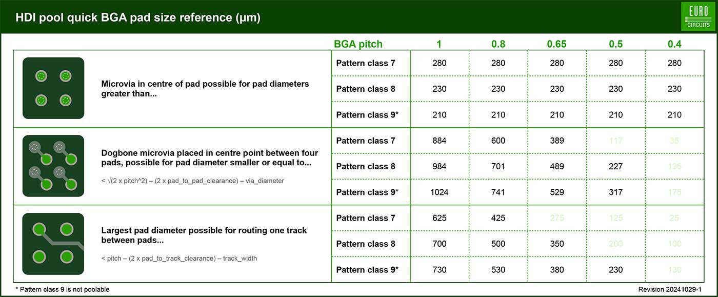
It’s also useful to know early on if dogbone pattern routing, and having tracks between pads, will be possible, and Figure 3’s second and third rows show the largest BGA pad diameters for achieving those.
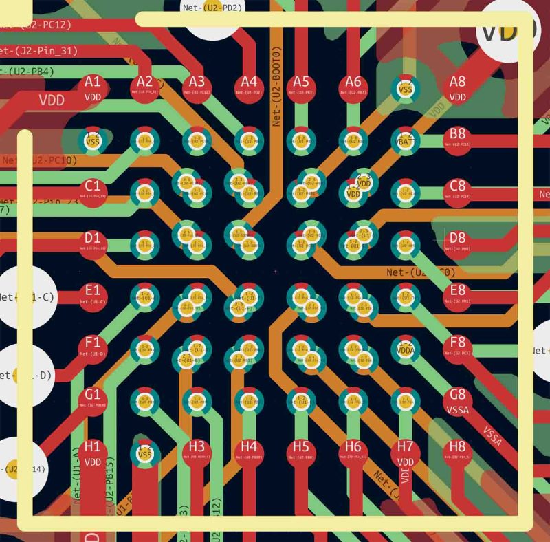
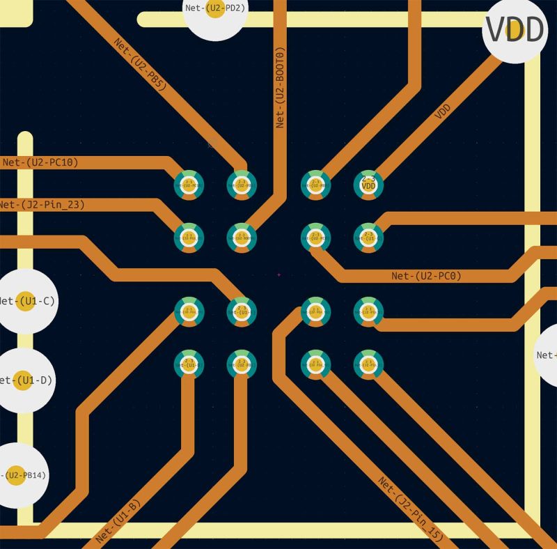
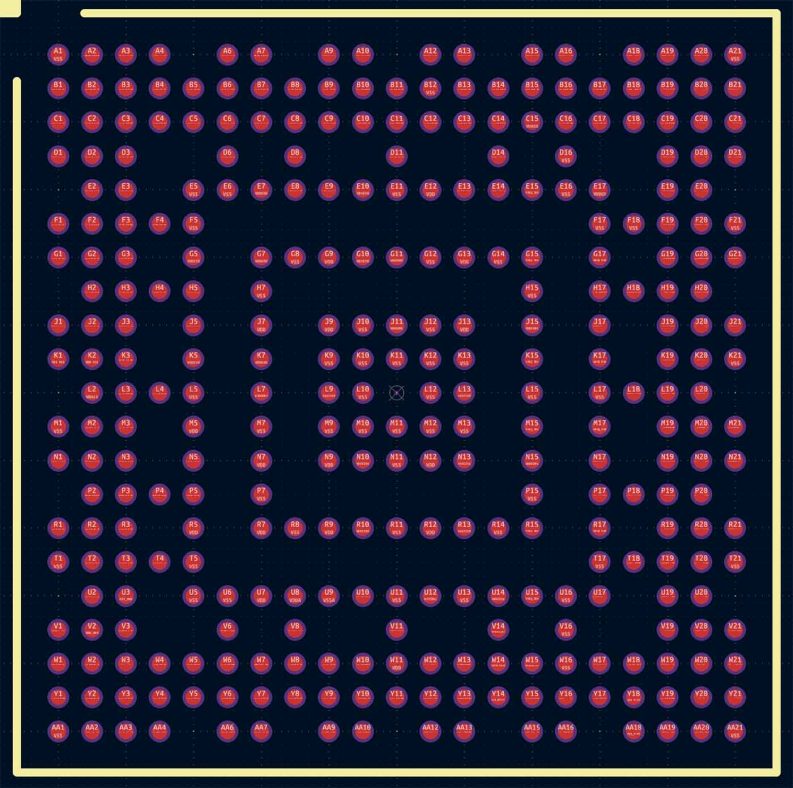
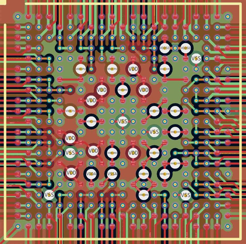
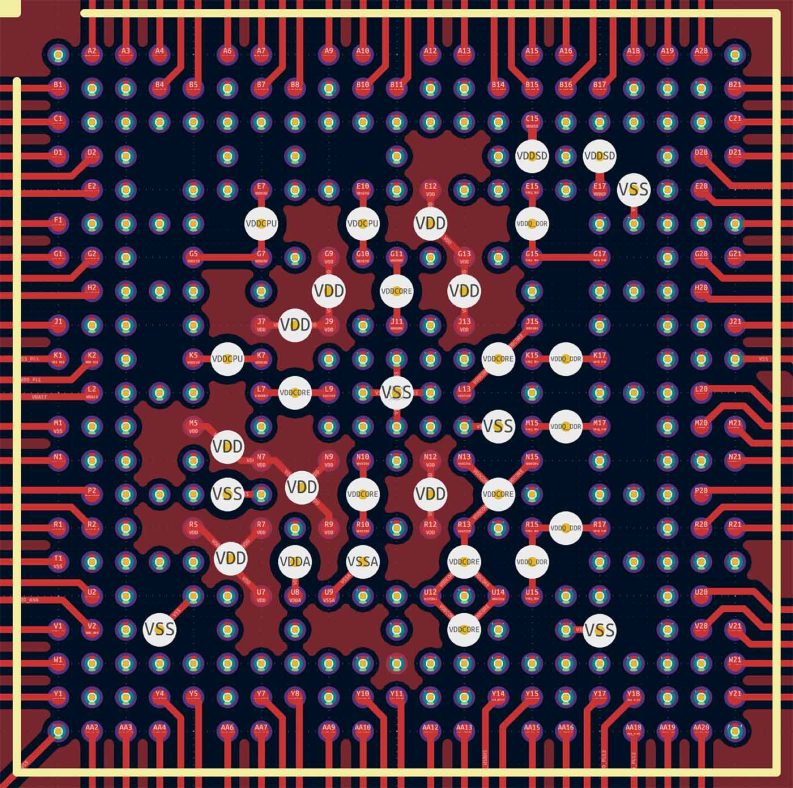
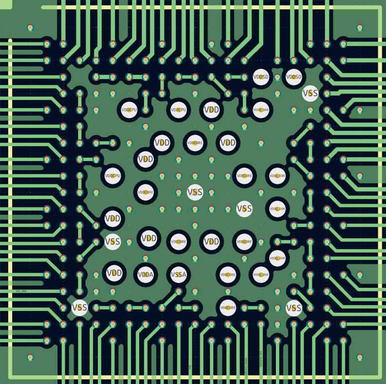
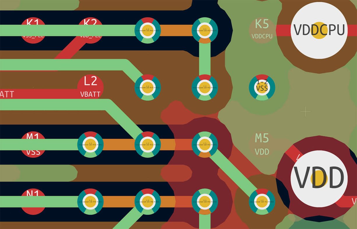
Let’s now consider an 8×8 BGA array. A basic routing strategy is to look at the BGA’s array ‘rings’, working from the outside inwards; the first ring is routed in L1, the second ring in L2 with L1-L2 microvias, and the third and fourth rings are routable in L3 using staggered L1-L2 and L2-L3 microvias. An example of a fully routed 8×8 BGA is shown in Figure 4 using our Pattern class 8 (with Drill class E for the through-vias).
There are a few additional things we can learn from this strategy. The L1-L2 microvias are in the centre of the pads – they happen to be of exactly the same diameter – and the L2-L3 staggered microvias are symmetrically ‘balanced’ by quadrants, helping us route the most inner ring between those microvias (shown in Figure 5). This arrangement is also very helpful for assembly where heat is more evenly distributed across the BGA pins such that the component is less likely to shift out of alignment.
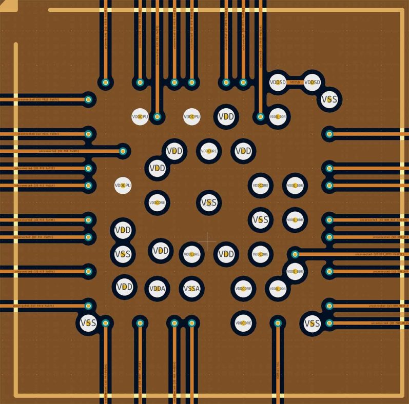
With a limit of two microvia runs, this strategy doesn’t necessarily scale if we want to route all pins of a full BGA array greater than 8×8 or 9×9. However, there are several factors that will make it possible, even for much larger arrays. For this let’s consider a 320-pin 0.5 mm pitch BGA shown in Figure 6, and its fanout in Figure 7.
As before, we route the outermost rings on L1 (Figure 8), with the helpful placement of power and ground pins, and pin gaps, routed using through-vias (0.5 mm pads with 0.15 mm hole, so Drill class D). The routing of the next few rings are shown in Figure 9 together with the routing between the L1-L2 and L2-L3 microvias, the latter also placed in the pin gaps (Figure 10), and finally, the rest of the signals are routed in L3 (Figure 11).
It’s important to note that in our examples, all pins were fanned out, but many designs don’t use all the pins of a package, which may make routing easier. So whilst our HDI pool parameters were chosen to allow the full routing of most 8×8 BGA arrays, we are confident that larger arrays are also possible in real-world designs!
The best next step is to get familiar with the HDI pool through the Visualizer. And the next best thing is to upload a design to test how well the HDI pool can help with cost reduction of your BGA boards.