The Advanced options section allows you to select from a range of additional options to be applied during the manufacture of your PCB(s).
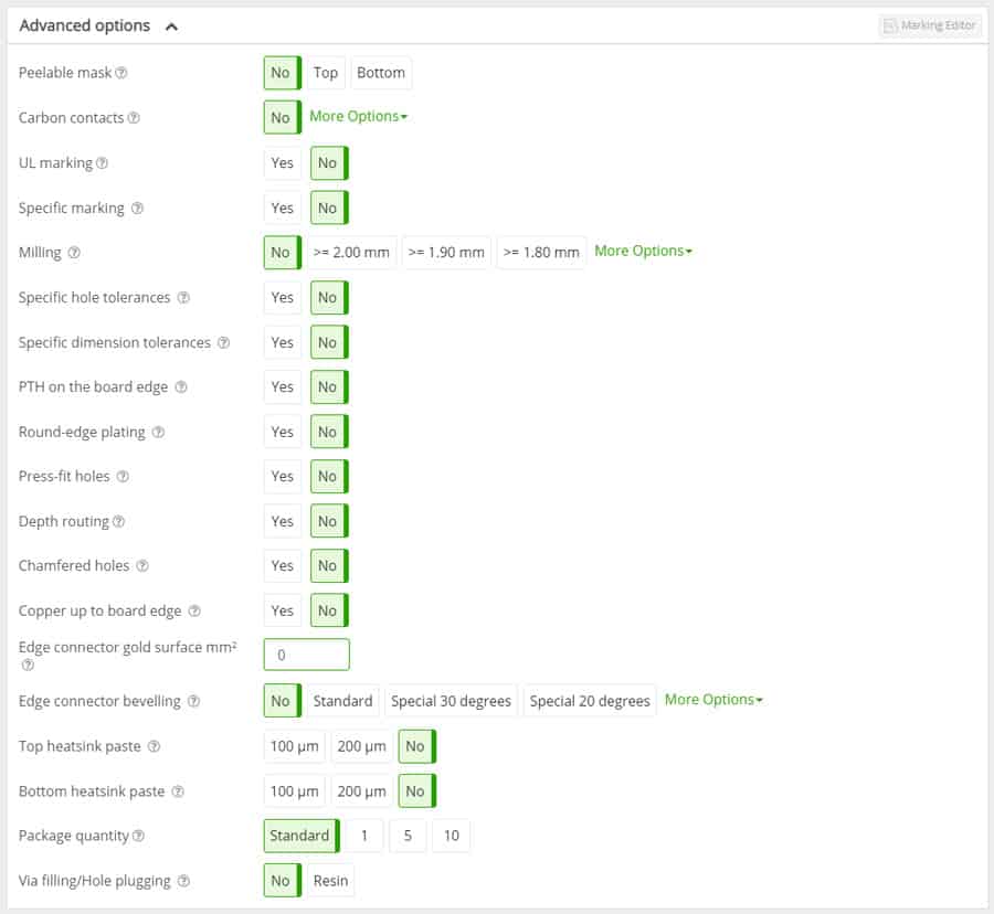
IMPORTANT
- Selecting any of these options may increase the price of your PCB.
- Selecting some options will trigger a warning to update or change parameters/values lin other sections, see example below:
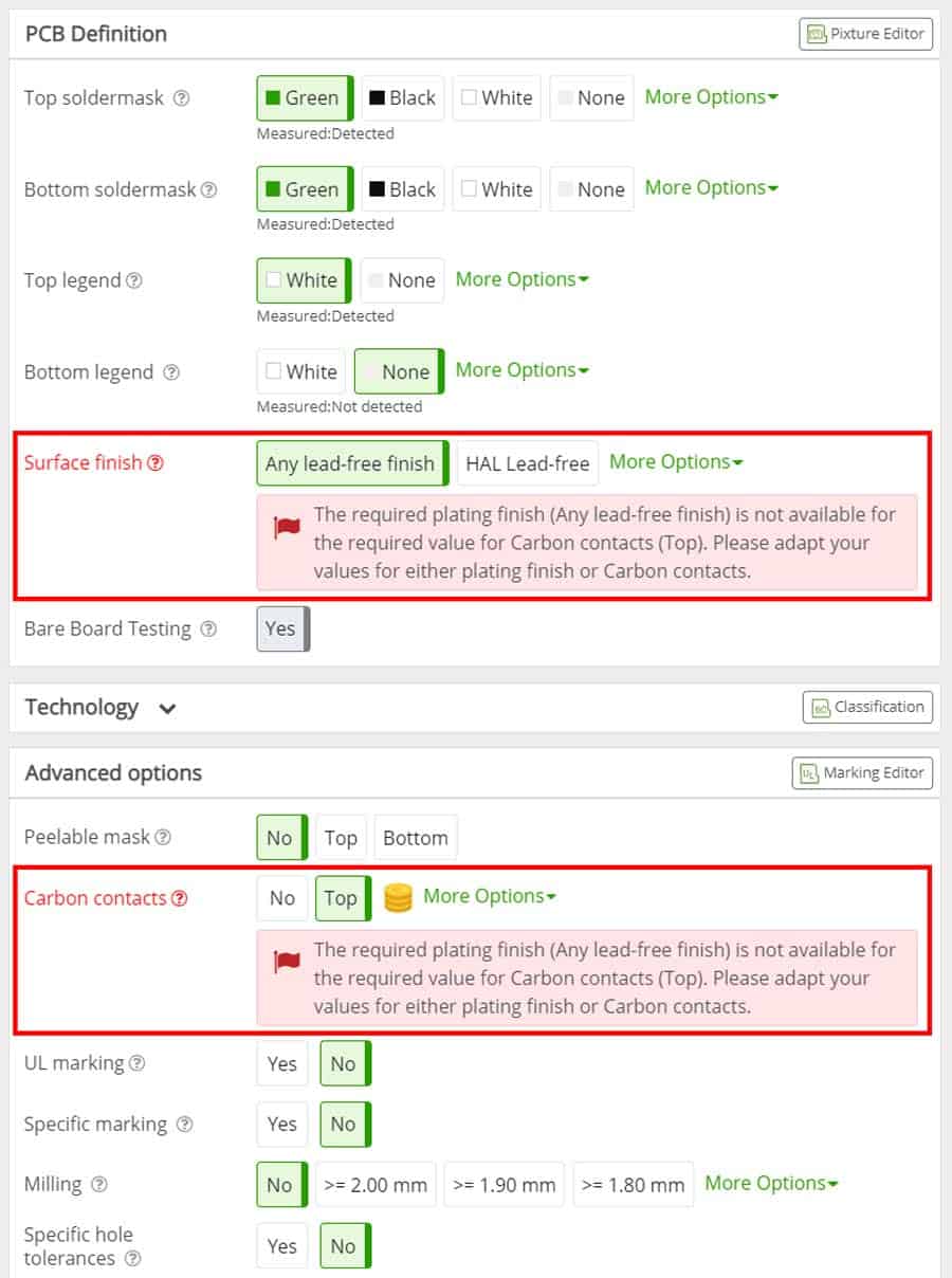
By selecting Carbon contacts, a warning has been triggered, the same warning will also appear in the row of the parameter where the selected value needs to be changed.
Peelable mask
Default – No
If a peelable mask is require please select whether it is required on the Top or Bottom side of the PCB.
NOTE
- If selected it may trigger a warning message.
See also:
PCB Design Guidelines – Peel-Off Mask
Carbon contacts
Default – No
If carbon contacts are required, please select whether it is required on the Top or Bottom or Both sides of the PCB.
NOTE
- If selected it may trigger a warning message.
See also:
PCB Design Guidelines – Carbon Contacts
Carbon Conductive Ink Technical Data Sheet
UL marking
Default – No
If a UL marking is required on the PCB, please select Yes.
Please use the Marking Editor to select the location where the UL marking should be placed.
See also:
Our UL Certifications
What About Underwriters Laboratory (UL)?
Specific marking
Default – No
If one or more specific marking (e.g. – date code) is required on the PCB, please select Yes.
Please use the Marking Editor to select the location where the specific marking(s) should be placed.
See also:
What are Specific Tolerances?
Milling
Default – No
The standard tool diameter for milling is 2.00mm, if you require a smaller tool diameter please select one from the options available.
See also:
PCB Design Guidelines – Mechanical Layer
Finished Slot Size Tolerances
What is Milling or Routing?
Sorting out Drills and Cutouts
Specific hole tolerances
Default – No
If your PCB(s) require hole tolerances other than the Eurocircuits standard hole tolerances please select Yes.
NOTE
You must also provide additional information on the require hole tolerances and to which drilled holes they apply too.
See also:
PCB Design Guidelines – Drilled Holes
Finished Hole Size Tolerances
Specific dimension tolerances
Default – No
If your PCB(s) require dimension tolerances other than the Eurocircuits standard tolerances, please select Yes.
NOTE
You must also provide additional information on the require dimension tolerances.
See also:
PCB Design Guidelines – Mechanical Layer
Specific Tolerances
PTH on the board edge
Default – No
If your design includes plated through holes on the edge (contour) of the PCB, please select Yes.
See also:
Plated Holes on the Board Edge
Copper and the Board Edge
Round-edge plating
Default – No
If you require the edges of your PCB(s) to be plated, please select Yes.
NOTE
- If selected it may trigger a warning message.
See also:
Copper and the Board Edge
PCB Design Guidelines – Copper Layers
What is Round-Edge Plating
Press-fit holes
Default – No
If you design requires specific holes to be press-fit, please select Yes.
NOTE
You must also provide additional information to identify which holes are press-fit.
See also:
What are Press-Fit Holes
Depth routing
Default – No
If your design requires depth routing, please select Yes.
NOTE
You must also provide additional information including dimensions for each individual area of the PCB that requires depth routing.
See also:
What is Depth Routing
Chamfered holes (Countersunk)
Default – No
If your design requires chamfered (countersunk) holes, please select Yes.
IMPORTANT
We can only offer chamfered holes for standard M3 screws.
NOTE
You must also provide additional information to identify which specific hole(s) on the PCB are to be chamfered.
See also:
What are Chamfered Holes
Copper up to board edge
Default – No
If you require copper to the board edge, please select Yes. The standard procedure is to remove all copper 0.25 mm from the board edge.
See also:
Copper up to the Board Edge
PCB Design Guidelines – Copper Layers
Copper and the Board Edge
Edge connector gold surface mm2
Enter the total edge connector gold surface (mm²) for both the TOP and BOTTOM layers of the PCB.
See also:
Edge Connectors with Gold Surface
Gold Plating for Edge Connectors
Edge connector bevelling
Default – No
If bevelling for the edge connectors is required, please select the required angle from the options available.
See also:
What is Edge Connector Bevelling
Plated Gold Edge Connectors
Edge Connectors with Gold Surface
Gold Plating for Edge Connectors
Top heatsink paste
Default – No
If you require heatsink paste to be applied to the TOP layer of your PCB(s) then please select the required thickness from the available options.
See also:
What is Heat sink Paste
PCB Design Guidelines – Heatsink Paste
Bottom heatsink paste
Default – No
If you require heatsink paste to be applied to the BOTTOM layer of your PCB(s) then please select the required thickness from the available options.
See also:
What is Heat sink Paste
PCB Design Guidelines – Heatsink Paste
Package quantity
Default – Standard
Our standard quantity of PCBs shipped in one package is ????, if you require a different package quantity then please select the quantity from the available options.
Via filling/Hole plugging
Default – No
Completely closed via holes can only be guaranteed by using Via Filling. We can offer Via Filling with resin – a non-conductive material TAIYO THP-100DX1.
Please select Resin if you require Via filling for your PCBs.
NOTE
You must also provide additional information to identify which specific via hole(s) on the PCB are to be filled with resin.
See also:
PCB Design Guidelines – Via Filling
What is Via Filling
Covering vias