Good courtyards make good neighbours
We continue our series on PCB design and manufacturing topics; this is the second article of six. Please follow us on social media or sign up to our mailing list to continue getting our publications. Now for today’s topic!
When designing boards we naturally first focus our attention on electrical functionality. But we also need to eventually manufacture the thing and that brings considerations that are better addressed as early as possible in the design process. Courtyards are an important design tool that help us make sure our boards will be manufacturable in a consistent and reliable way.
What are courtyards and why we need them
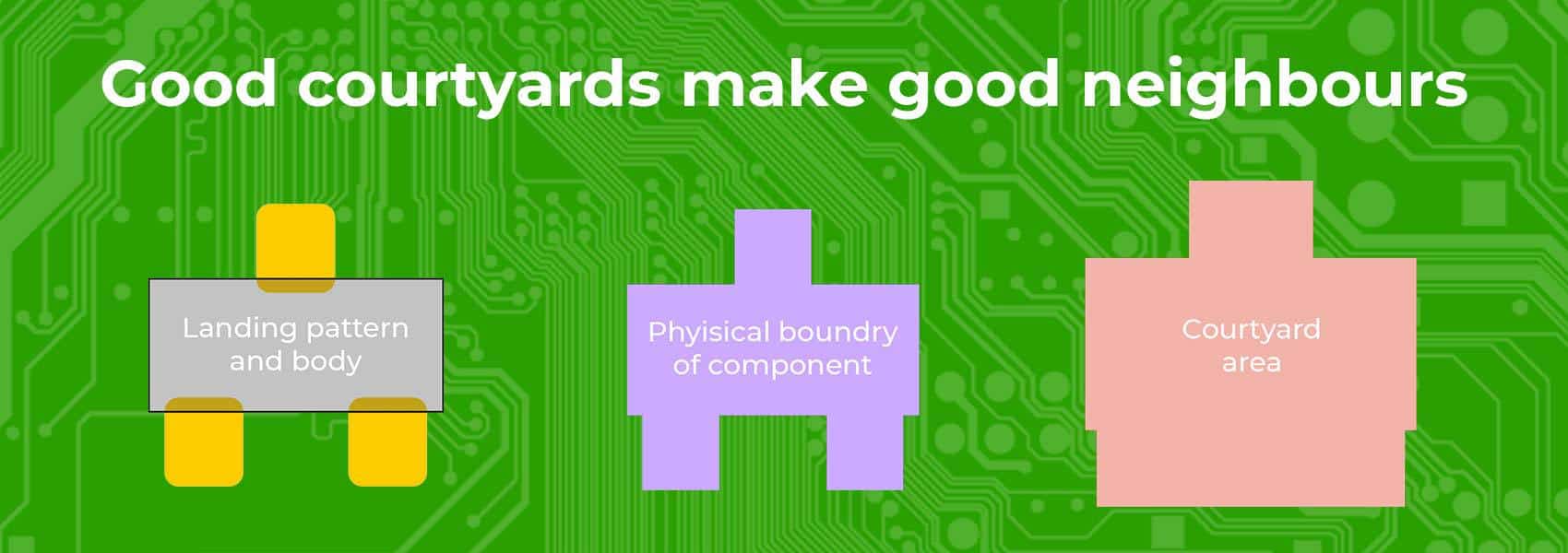
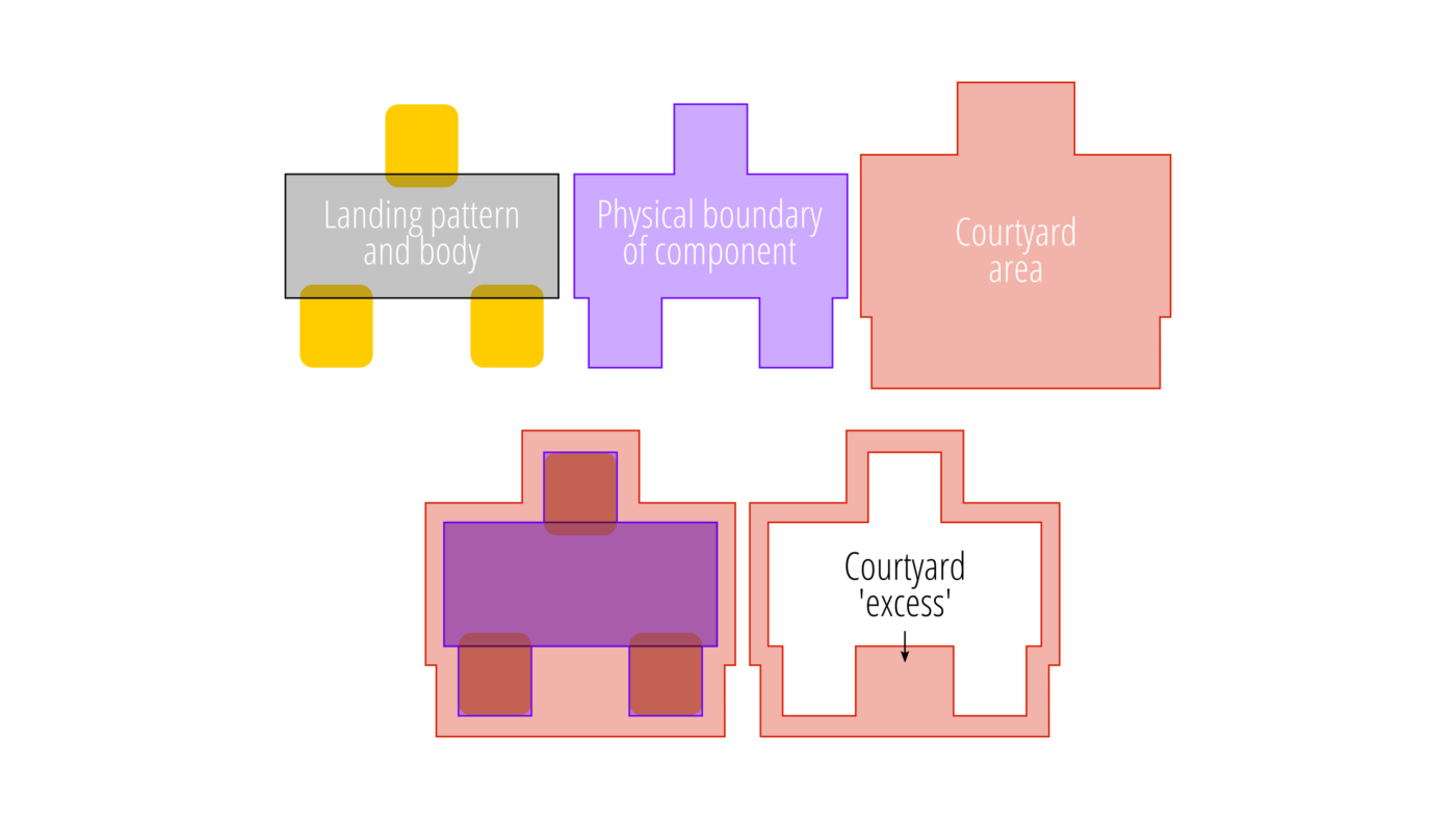
A courtyard is a virtual area defined at a certain distance from the physical outline of a component. It is created at the component-level as part of its footprint definition and is used to tell our design tools where no other courtyard should enter.
Here are a few reasons why we’d want to have space around components that’s free of other components:
- Most PCB manufacturing steps have a certain registration tolerance where alignment might not be perfect; this is a fact of any manufacturing process. Allowing room for the worst case mis-registration combination makes sure that we won’t have components clash across many manufacturing runs.
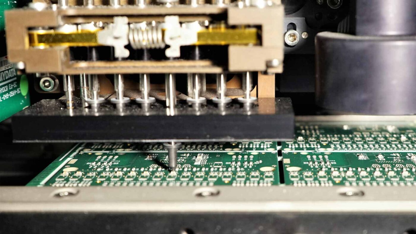
- The assembly heads that pick-and-place components need to maneuver into tiny spaces where components that have already been placed might be in the way; having more room allows them to do that without potentially banging into them.
- Space helps optical inspection to detect issues after assembly.
- More room between components help reduce heat density by allowing increased airflow.
- Sometimes large components cast a shadow over smaller components placed next to them. This can cause ‘cold spots’ where solder paste is slow to melt compared to other areas of the board during assembly resulting in faults.
- Finally, if we need to do some rework, more room is always appreciated!
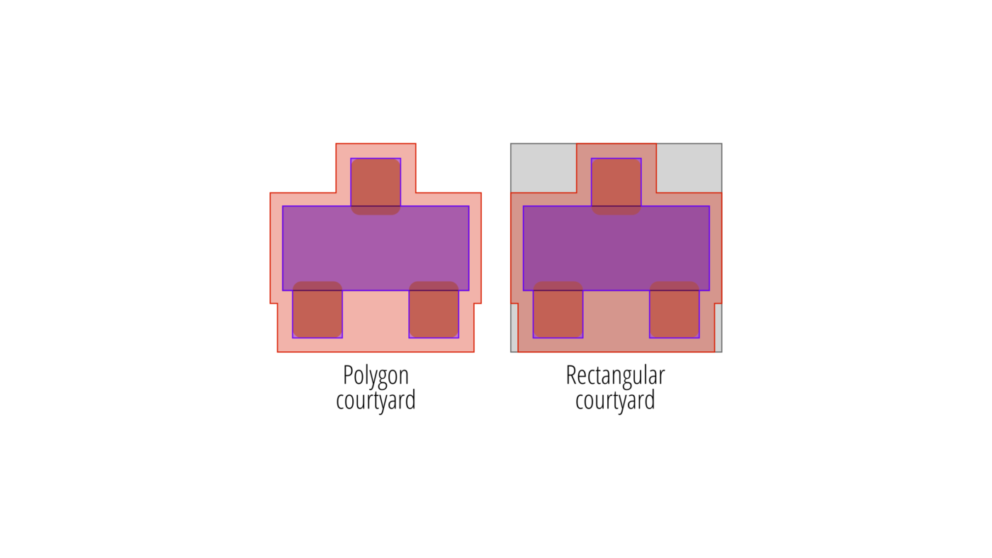
In IPC-7351B the IPC defines courtyards as “the smallest rectangular area that provides a minimum electrical and mechanical clearance (courtyard excess) around the combined component body and land pattern boundaries”. But rectangles aren’t very good as they can ‘consume’ too much space around a component, like the corners of a QFP that could be used for placing passives. My understanding is that the draft version ‘C’ of the spec uses the more effective ‘polygons’, although the industry seems to already be there in terms of how courtyards are used in practice.
The IPC’s specification for how large the courtyard needs to be depends on three different component density levels. But we should remember that the IPC provides guidelines that are somewhat conservative because they are meant to apply to as wide a range of equipment capabilities as possible. So in reality, and also according to the IPC, the actual dimensions of courtyards is determined by the specific machines we’ll use, our own hand-soldering dexterity, or even the particular location a component is placed in relation to others on the board.
Using courtyards effectively
The effectiveness of courtyards hinges on two things. On the designer who needs to define them meticulously, and correctly set up the EDA tools’ Design Rule Checkers (DRCs). And, on the DRCs ability to actually detect all the issues. These settings need to be reconciled with the manufacturer’s specifications to make sure that they’re not in conflict.
But there’s subtlety here. When we put two identical components next to each other and just butt their courtyards together, we effectively double the courtyard distance. In that case we’ll need to know what the courtyard is protecting us from in the list above, and how manufacturer-specific we’re designing for. If we want a board that can be manufactured anywhere, sticking to the IPC rules is a good idea. But while we might get a DRC violation on the EDA side for courtyard violations, from the manufacturability point of view it’ll be just fine. All of this can become painful when going from prototype manufacturing at one place to production manufacturing elsewhere… a redesign. It’s worth thinking about it all as early as possible!
Some designers choose to use the component’s legend layer as a pseudo-courtyard definition but I think that that’s a bad idea. Here’s why:
- The DRC won’t catch any problems so you lose one of courtyards’ primary benefits.
- There is a minimum limit on the stroke thickness of silkscreen that’s quite wide in the context of tiny components we now design with. This means that on screen it’s a dominant, distracting, and inaccurate feature.
- Registration of the legend isn’t as tight as the copper or soldermask layers so it will look messy and illegible on the physical board.
- As boards become denser there’s not much room for a legend and these visual elements are one of the first to go when space is tight.
To sum up, we should not use a visual element with a DRC-able constraint. Invariably as the design progresses these elements will conflict and then both lose their effectiveness and purpose. Avoid it. Spend the time to define courtyards when you create the footprint and get the benefits of DRC and free up the legend for what it is intended for.
How our Visualizer helps
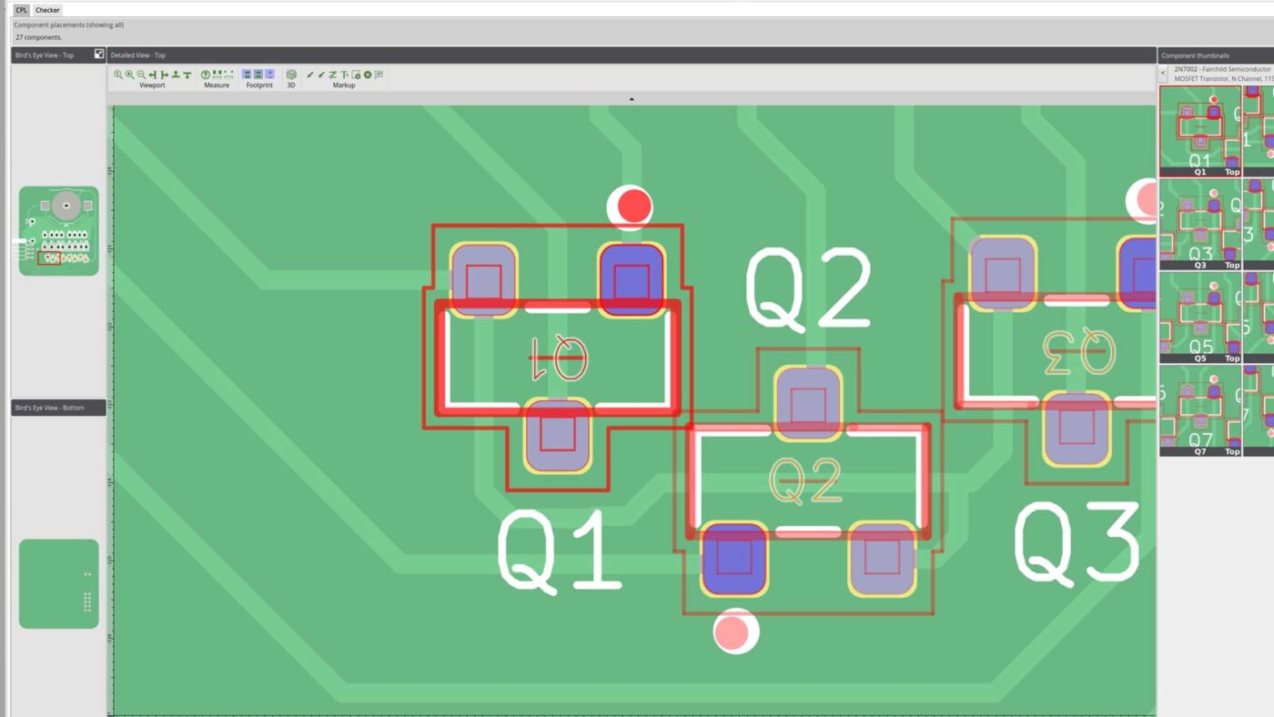
Our PCB Visualizer is a powerful tool that you’ll use when you order a board from us. It helps both you and us get it ‘right the first time to manufacture’. As always you can start by using it as your ‘external’ viewer to see if any glaring problems stare back at you.
Our Assembly Visualizer can evaluate the correctness of your footprints when you upload a Bill of Materials (BOM) and Component Placement List (CPL), and if it has the footprint in its database. It will also tell you if there are courtyard issues that will prevent us from assembling the board. If the Visualizer doesn’t have the footprint in its database, it won’t be able to check the correctness of your footprint. For this reason, if it’s possible for your design, try using components that we have in our database.
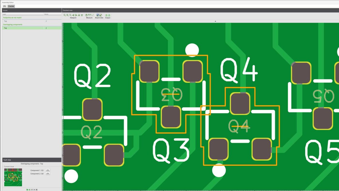
Our Visualizer will warn you if we cannot manufacture the boards, and will indicate if the placement of the components are compliant with IPC specifications for courtyard violations. It’s important that you make sure that the courtyards are correct for the capabilities of both your prototype and production manufacturers’ capabilities in order to avoid a redesign.
Here are our resources for the specs that are relevant to what we’ve discussed so far:
- Component clearance
- Cold and hot spots
- Gerber X3 component information contains a courtyard field
- Fine-pitch components
Bring your product to market on time and within budget – join the Eurocircuits Community


![]()

