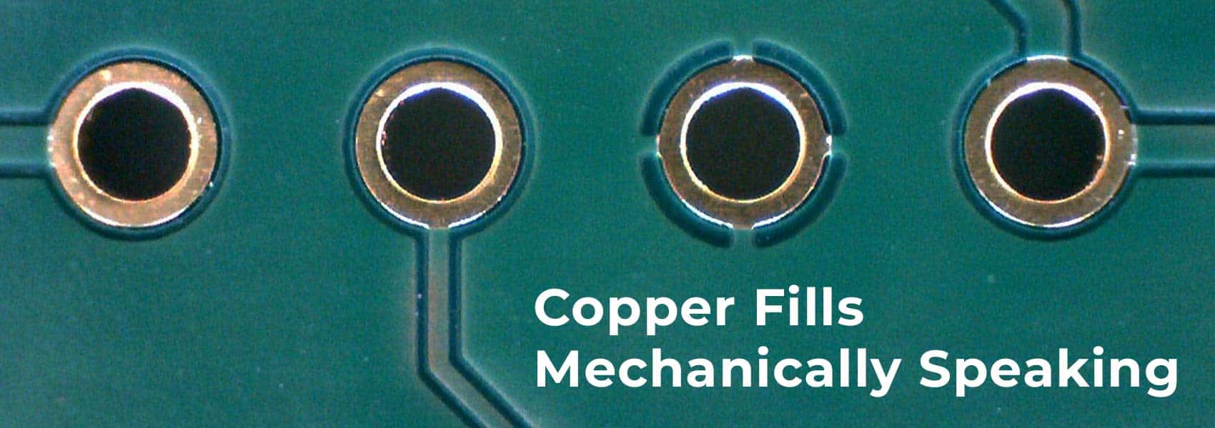
Copper fills – mechanically speaking
This is the sixth and final article of this series about PCB design and manufacturing topics. I hope that you’ve enjoyed it and will continue to follow up on our other publications until we return with series 2!
Copper fills — or copper pours — are one of those topics that’s deceivingly simple, but their use requires a great deal of consideration, both electrically and mechanically. How to use copper fills appropriately for high-speed digital design is a complex topic that I won’t even touch here. Instead, I’ll discuss the mechanical and manufacturability considerations.
A copper fill is pretty descriptive: fill an area with copper while keeping a defined distance from other copper features. The copper fill can be connected to a particular electrical net in order to carry and distribute a signal throughout the area it covers; usually those are power or ground but it can be any signal. Other copper features that are part of that same net are connected to the fill with copper, while the rest are not.
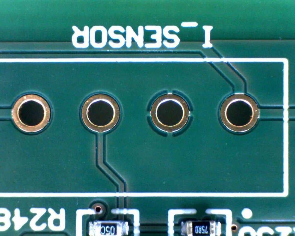
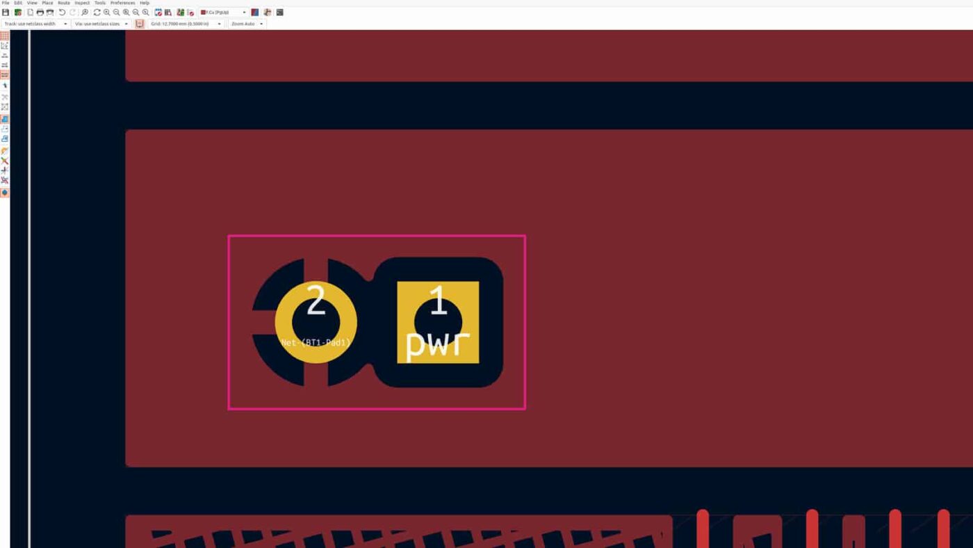
Copper is a good heat conductor, so any local heating is quickly distributed across it; this means that fills behave like thermal sinks. Sometimes this is desirable, like when dissipating heat from a component’s large ground pad, but it’s not something you want when trying to localise heat onto a pad while soldering. The most common way to avoid that sink is to use a thermal relief where bridging tracks, or spokes, are added between the pad and the fill in order to reduce heat dissipation. That way, more heat remains in the pad for long enough to make soldering easier, faster, and more consistent.
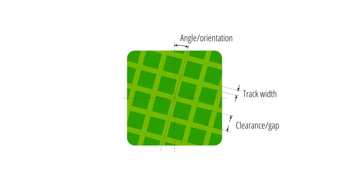
Design tools normally have two ‘fill’ options: solid or hatched. Solid fills are the most common; calculations for impedance and return paths are straightforward and they do not complicate the manufacturing process as we’ll discuss later. Solid fill should be our default.
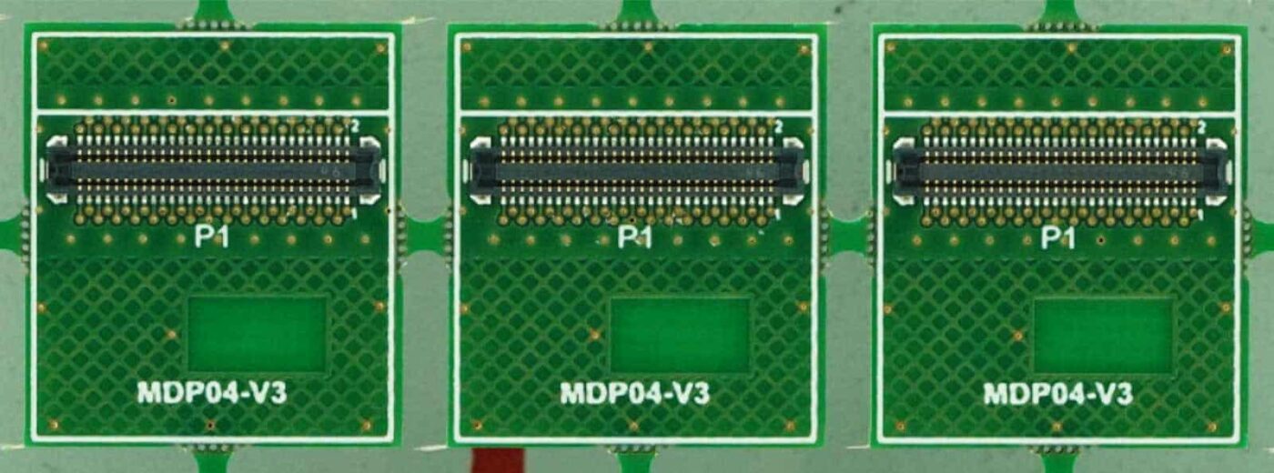
In the distant past, hatched fills were often required to help adhesion of copper, resin, and soldermask onto the base material so that they don’t ‘delaminate’ during or after manufacturing. Modern processes do not require hatching for reliable PCB manufacturing, so there is no need for a hatched fill except maybe in some cases listed below. (By the way, if a fab does require hatching, check if they might be using very old equipment and manufacturing processes.)
- Some chip manufacturers suggest a hatched pattern around capacitive touch pads.
- Hatched patterns may provide more physical flexibility in very thin boards.
- Creative signal integrity gymnastics in unique circumstances (like very thin boards or exotic substrates) may require a non-solid pattern.
- Hatched patterns reduce the copper density on the board to expose more of the substrate, which may sometimes be required for balancing the copper. A good manufacturer should be able to tell you if parts of your solid pattern should be replaced with a hatched for this reason.
- If you’re designing a beautiful circuit, a hatched, or even a more elaborate pattern, might be a requirement for visual effect. In this case, talk to your friendly fab fab that this is something they’ll take on and learn about the constraints in which you must operate… not everything is possible.
There are probably more cases, but they’re probably even more esoteric. So stick to a solid fill unless you can really justify using any other pattern. And, as always, it pays to talk to your manufacturer early on. (As a side note, the wonderfully-open-source KiCad’s next release, v6, will add an option for a hatched fill… don’t be tempted!)
The problem with hatched and other patterns
Hatched patterns are a headache for manufacturers. That’s because a lot of verification happens on the data we submit before it goes to manufacturing, and hatched patterns make some of those checks significantly more demanding and time consuming than if fills were solid.
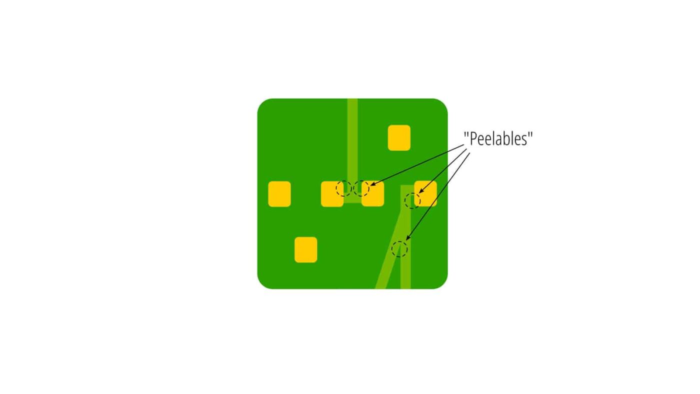
Peelables (not to be confused with peel-off/peelable soldermask) are areas where features of the same net create a tiny sliver or corner. During manufacturing we cover the areas of copper that we want to be removed with dry film, or photoresist. Then we plate the panels with electrolytic copper and tin and etch in treatment baths. If during this process tiny bits of film detach, float around, and reattach themselves elsewhere on the panel they can cause circuit shorts, opens, and imperfections. To help prevent this, we search for peelables and repair them, but with a hatched pattern there can be many more than usual.
Pinholes are tiny holes in what otherwise looks like a solid plain; this is often caused by design tools approximating solid shapes, like a fill, with stroked segments or polygons. As with peelables, these pinholes can cause issues when tiny dry film pieces that cover them detach, float, and reattach elsewhere on the panel. We look for and fix pinholes by ‘filling’ them with copper in the design files. And, as before, hatched patterns have the potential of creating many such pinholes instead of the occasional few with a solid fill.
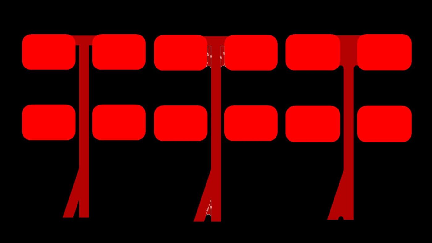
Performing general DRC on a hatched-filled board is very demanding to verify. Stroked-track distance violations are easy for the tools to find, but much harder to impossible to find if they happen within a single shape. One example of this is what we call copper cuts: tiny connections between two large same-net copper features that aren’t a track; If we don’t detect and fix these, they will be over-etched and disappear.
So while detecting and repairing potential problems with hatched patterns is possible, it comes at a cost in processing time by the CAM software, and the cost of engineers who operate and monitor them. That obviously increases production costs. Some of that higher cost is transferred to the customer, but the primary to the customer impact are delays in processing the data and then fixing it. Ultimately, a good design is manufacturable consistently across several manufacturers, and a hatched fill may introduce too many unwanted variations to achieve that.
How the Eurocircuits way helps
When you submit a board to be manufactured by Eurocircuits our priority is to make sure that it can be manufactured reliably. We go to great lengths to make sure that this is the case so that you get back high-quality boards as fast as possible. To do this we fix problems in the data that we know may cause issues, like peelables, pinholes, and copper cuts. Unfortunately, dense hatched fills cause a lot of these things to happen much more frequently than if they are not used.
All that said, we can manufacture hatched fills if it’s required by your design. They need, however, to meet a minimum density specification:
PCB Design Guidelines – Copper Layers
If the hatched pattern does not meet these minimum requirements it will be converted to a solid fill.
Here are our resources for the specs that are relevant to what we’ve discussed so far:
Bring your product to market on time and within budget – join the Eurocircuits Community


![]()

