Applying Carbon Contacts to PCBs

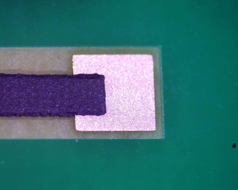
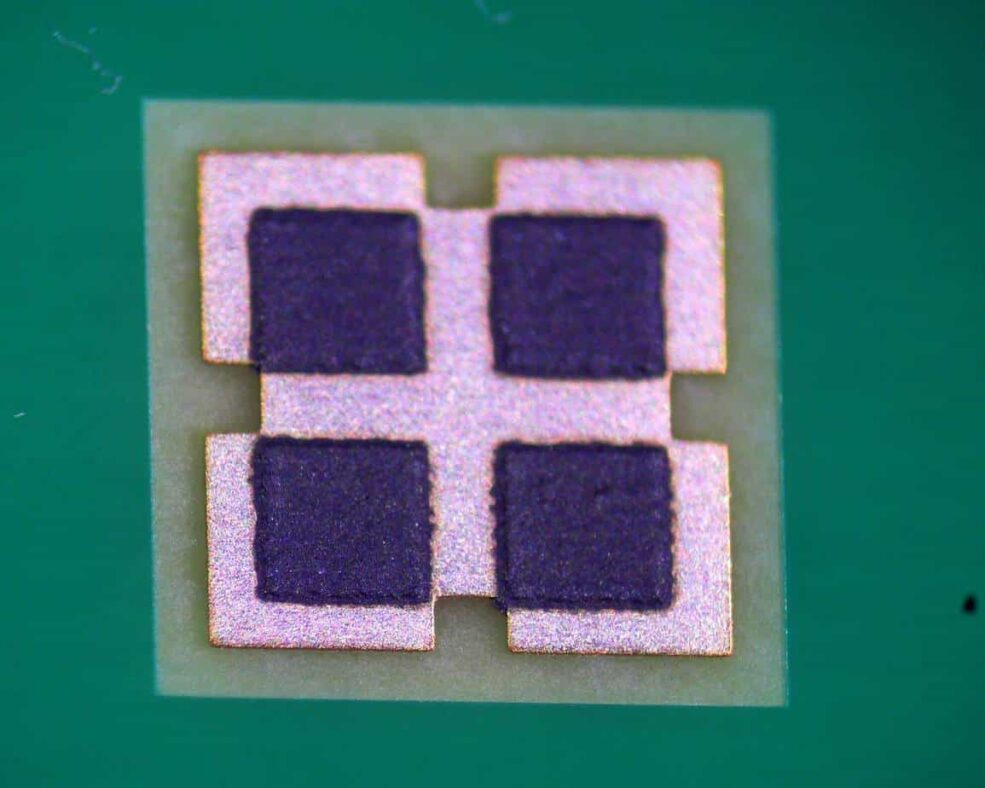
Conductive carbon ink is added to a finished PCB in order to provide a robust and long-lasting electrical interface with another mechanical component, such as a key or dial. It does that in two main ways: it raises the shallow copper contact above the surface of the PCB; and, it protects the PCB contact from oxidation, contaminants, and debris.
Carbon ink also has a defined resistance per area so it is a way to create ‘printed resistors’, particularly ones of non-standard shapes and sizes that can be used with dials and other mechanical interfaces. Conductive carbon ink is hardened by ‘baking’ and will maintain its properties (resistance, shape, conductivity) after the reflow of the PCB during assembly.
Carbon contacts at Eurocircuits
We apply conductive carbon ink using screen-printing, following this process:
- Apply the pattern onto a polyester fabric screen; this is done by applying a photosensitive film and mask, and then UV curing.
- Place the PCB panel and screen in the screen printing machine’s frame.
- Adjust the screen and panel according to matching reference marks.
- Set the squeegee pressure and speed settings which affect the carbon’s thickness.
- Cover one panel with a sticky transparent foil and perform a test print run and fine-tune for alignment if necessary until it’s within our tolerances.
- Remove the transparent foil and perform the actual carbon print on the panel.
- Cure the panel for 45 min at 150°C.
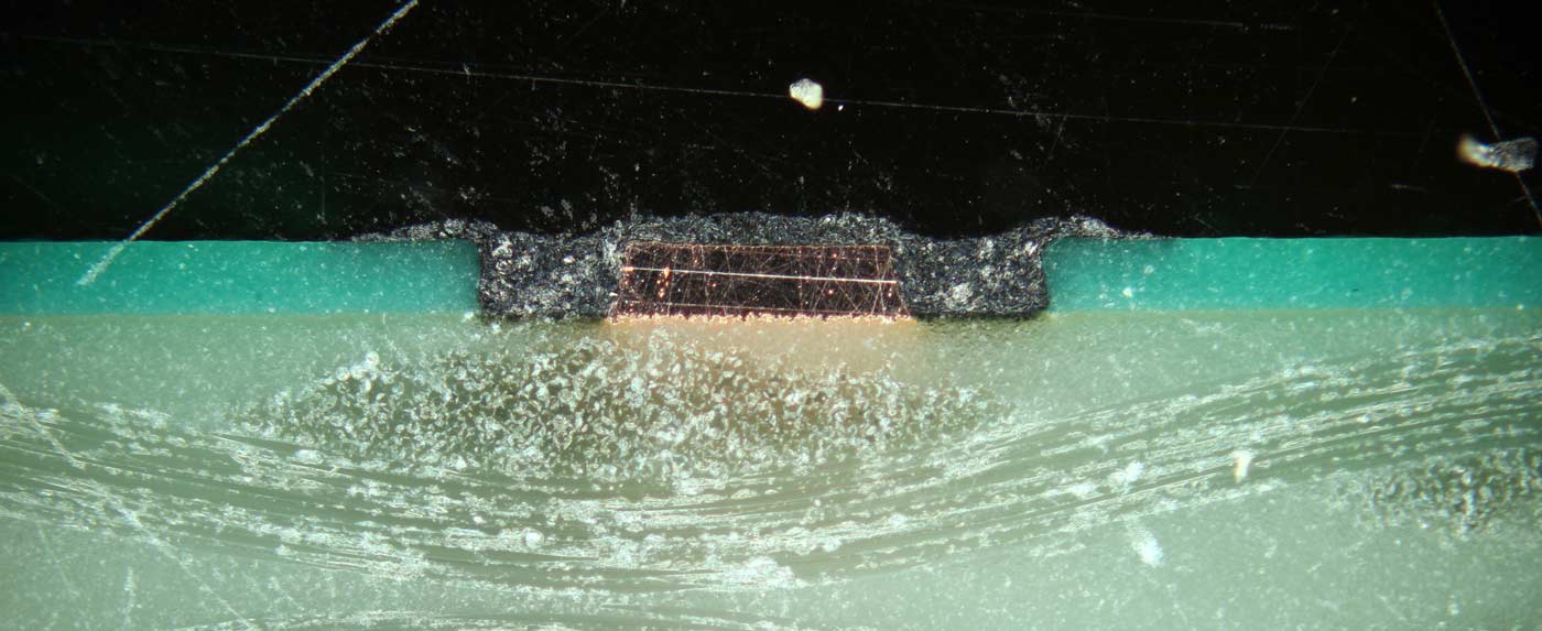
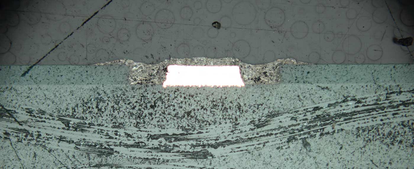
- Check the carbon surface for imperfections and measure its resistance.
The datasheets for the carbon-conductive ink is available on our Downloads page; they specify all the properties of the ink that could be relevant to an application (such as resistance per area, etc.) Our design guidelines for defining carbon contacts in your data, and manufacturing tolerances are at PCB Design Guidelines – Carbon Contacts.
Bring your product to market on time and within budget – join the Eurocircuits Community


![]()

