Many parameters in PCB design seem simple. But in practice they are far more complex than they appear at first glance. Saar Drimer, electronics designer and technical editor, explains these parameters with examples and shows potential pitfalls. In this 6-part series, Saar also gives valuable tips for a good PCB design that any manufacturer can produce.
Enjoy your reading.
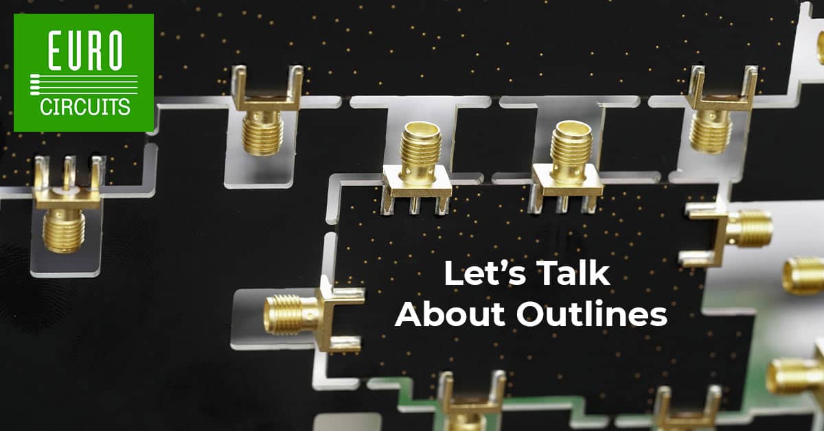
The outline must have a closed shape
Normally, the centre of the line thickness of the outer contour is used as the actual outline of the PCB. This sounds simple, but this is where the mistakes lie.
Read more…… |
 |
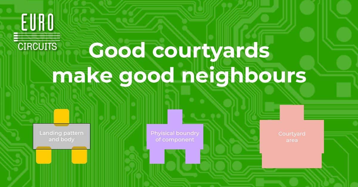
Courtyards create safety spacing for the components
The courtyard defines a safety spacing around a component similar to a fence. In this article, Saar shows how to use courtyards effectively.
Read more…… |
 |
Annular rings: the correlation of hole diameter and copper pad
In practice, we have two diameters for the plated-through hole: the actual hole diameter and the finished hole diameter.
Read more…… |
 |
Keepout areas protect against costly errors
Keepouts are areas on the PCB where we instruct our design tool to enforce restrictions on what is and is not allowed in that area.
Read more…… |
 |
Fiducials must be reliably detected
The geometry and placement of the fiducials determines the reliability of the PCBs to be produced. Here are our tips.
Read more…… |
 |
Solid copper fills are the first choice
This article explains the mechanical and manufacturing aspects of copper surfaces for PCB designers.
Read more…… |
 |