User Guides
Our User Guides provide step-by-step instructions on how to use our free online smart tools and other available software.
The copper thickness of the layers of a Printed Circuit Board varies depending on the material and manufacturing process.
When we consider the layer copper thickness on a PCB we refer to:
The IPC-4562 and IPC-A-600 define both the acceptable thickness and tolerances for both the Base and End copper.
Originally the base copper thickness was defined on the basis weight over an area, as in oz/ft² (oz = ounce and ft = feet) however, today it is more commonly defined as an actual thickness measurement, for example 35 µm.
So how do we convert oz/ft² to an actual measured thickness?
This is done by theoretically spreading the oz value of copper evenly over 1ft² and then measuring the thickness of the copper.
For example, 1oz/ft² has a thickness of 1.37 mil (0.00137 Inch) or 34.798 µm (0.034798 mm).
As with all things that are manufactured there is Manufacturing Tolerance that we must take into consideration. The IPC-4562 standard allows for up to a maximum of 10% reduction in the base copper thickness as supplied by the base material manufacturer.
This means 34.798 µm (35 µm) is allowed to be a minimum of 31.31 µm thick.
Table 1: Base or Start Copper Thickness
Imperial |
Actual Conversion |
Industry Defined Thickness |
| 3/8 oz | 11.599 µm | 12 µm |
| 1/2 oz | 17.399 µm | 18 µm |
| 1 oz | 34.798 µm | 35 µm |
| 2 oz | 69.596 µm | 70 µm |
There are 2 methods for creating the tracks and gaps on a PCB, the first is print & etch and the second is pattern plate.
This method is mainly used for Inner layers without Blind or Buried Via Holes or PCBs that do not require Plated Through Holes (PTH).
Here the situation is much simpler as the final thickness of the inner layer copper is defined by the base copper as there is NO plating process required just some cleaning and micro etching procedures which will reduce the Start Copper a bit.
Table 2: Print & Etch – Start vs End Copper Thickness
Industry Defined Copper Thickness |
Start Copper Thickness |
Minimum End Thickness after Processing(IPC-A- 600J-Class 2) |
| 12 µm | 12 µm | 9.3 µm |
| 18 µm | 18 µm | 11.4 µm |
| 35 µm | 35 µm | 24.9 µm |
| 70 µm | 70 µm | 55.7 µm |
| 105 µm | 105 µm | 86.6 µm |
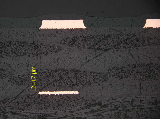
Inner Layers with 18 µm Start Copper
This method is used for PCBs with PTH or Inner Layers with Blind or Buried Via Holes or where thicker than available copper is required.
If PTH are present we plate the barrel of the holes using the Galvanic process with minimum of 18 µm of copper as defined in the IPC 600J-Class 2 standard however, Eurocircuits internal standards state that a minimum of 20 µm of copper should be plated on the hole barrel as this provides for increased quality and reliability.
To ensure connectivity a similar amount is plated on to the copper that will form the tracks after the etching.
Therefore, the “Start Copper Thickness” must be less than the required End Copper thickness.
During the various cleaning and micro etching processes the copper thickness is reduced. Plating increases the copper thickness. This plating process is influenced by the Copper Balance and Distribution (see our blog on the Plating Index) and unless this is uniform there will be a variation in amount of copper deposits across the PCB, basically it may be thicker or thinner in certain areas of the PCB.
Table 3: Pattern Plate – Start vs End Copper Thickness
Industry Defined Copper Thickness |
Start Copper Thickness |
Our Target Galvanic Plated Copper |
Our Nominal End Copper Thickness |
Minimum End Thickness after Processing(IPC-A- 600J-Class 2) |
| 30 µm | 12 µm | 20 µm | +/- 30µm | 29.3 µm |
| 35 µm | 18 µm | 20 µm | +/- 35µm | 33.4 µm |
| 70 µm | 35 µm | 20 µm | +/- 60µm | 47.9 µm |
| 105 µm | 70 µm | 20 µm | +/- 95µm | 78.7 µm |
| 140 µm | 105 µm | 20 µm | +/- 130µm | 108.6 µm |
Notes:
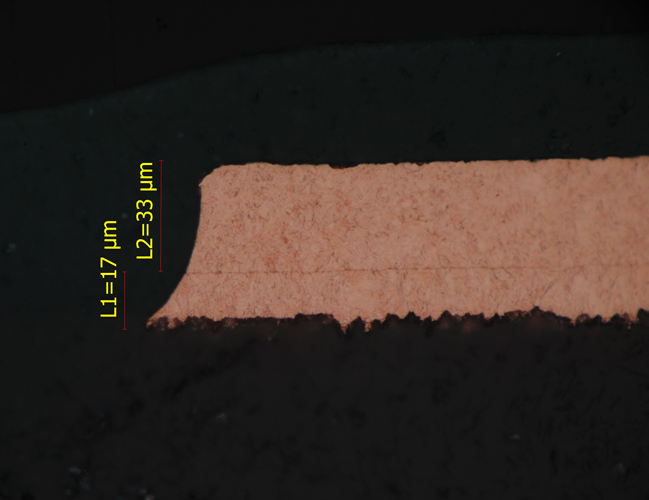 Outer Layer with 18 µm Start Copper |
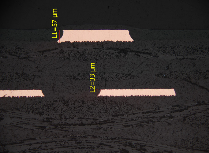 Outer and Inner Layers with 35 µm Start Copper |
In the our PCB Price Calculator you can select the copper foil which will be “Start Copper Thickness” as shown, next to this “Our Nominal End Copper Thickness” is shown. For example, 18 µm copper has an end copper defined as +/-35 µm.
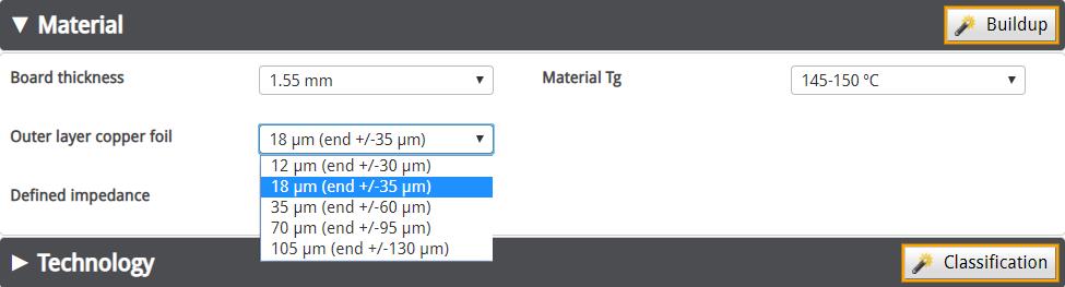
One question that might be raised is “what exactly does +/-35 µm mean?”. We also state these figures in the table above under the column “Our Nominal End Copper Thickness”.
But what does it mean, well there is no clear cut answer to this. According to the IPC-A-600J-Class 2 Standards an 18 µm Start Copper must have a minimum End Copper of 33.4 µm, here we state +/-35 µm as “Our Nominal End Copper Thickness” where the “+/-” means approximately and is based on our manufacturing experience but has a guaranteed minimum thickness of 33.4 µm
If we take a Start Copper of 70 µm it must have a minimum End Copper of 78.7µm under the IPC-A-600J-Class 2 Standards. Here we state +/-95 µm as “Our Nominal End Copper Thickness” again based on our manufacturing experience. The “+/-” again means approximately but has a guaranteed minimum thickness of 78.7 µm.
So why can’t manufacturers guarantee the End Copper thickness?
Simply put there are several factors that influence the End Copper thickness of a plated PCB, these include:
Our aim is always to deliver your PCBs as close to the required specification as possible and always within the allowable tolerances as stated by the IPC Standards.
To find out more about how we make cross sections please watch the short video below.