User Guides
Our User Guides provide step-by-step instructions on how to use our free online smart tools and other available software.
As with all manufacturing processes the Finished PCB Thickness is influenced by various factors and thus there is a tolerance applied to the final thickness.
The process of manufacturing a PCB starts with the Base Materials (e.g. FR4) and are available in various thicknesses.
The thicknesses available are nominal values and do not include the copper foil, basically just the laminate (resin and glass fiber weave).
These base materials also have a manufacturing tolerance applied to the nominal thickness.
This thickness tolerance is defined by the manufacturer in their data sheets.
For example, the typical thickness tolerance for FR4 is ±10% of the nominal value.
So a base material of 1.00mm may actually be somewhere between 0.90mm to 1.10mm thick (excluding copper).
For single and double sided PCB’s controlling the final thickness is less complicated, it’s mainly just the base material tolerance to take in to account.
For multilayers there are many for factors influence the final thickness of the PCB these are:
When you order a PCB’s you select a ‘Board thickness’ as below.
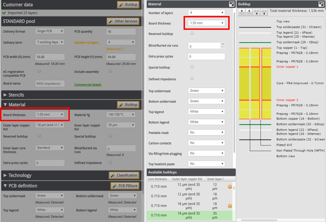
This is basically a label that our system uses to select the correct build-up for you your board.
The build-up is selected based on the Board thickness label, the number layers, type of material and copper thickness selected.
The actual calculated nominal ‘Total material thickness’ of the selected build-up is shown in the build-up window as below.

This is the total thickness of the base materials (laminate & prepreg) plus the selected copper thickness for that specific buildup.
This does not include the Copper Plating (Galvanic), Finial Finish Plating (Hal, ENIG etc.), Soldermask or Legend.
Our goal is to ensure that the thickness of the PCB is as close as possible to this selected value.
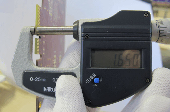
The thickness of a PCB must be measured on an area of laminate that is free of Soldermask, copper and legend.
Therefore, if you have defined your PCB to be 1.55mm thick then this is from the top laminate surface to the bottom laminate surface.
 |
 |
When designing your product for the location and fixation of your PCB you must take in to consideration the following:
All these values together form the total thickness of the PCB and this is as our customer is experiencing it.